Double pulse test

Minimizing switching losses remains a major challenge for developers of SiC and GaN-based power semiconductor devices. The standard method for measuring switching parameters and evaluating the dynamic behavior of Si, SiC and GaN MOSFET and IGBT transistors is the double pulse test (DPT). Using the double pulse test, the power losses during switching and de-switching of the component as well as the reverse recovery parameters can be measured.
Double pulse test and its advantages
The basics of the test
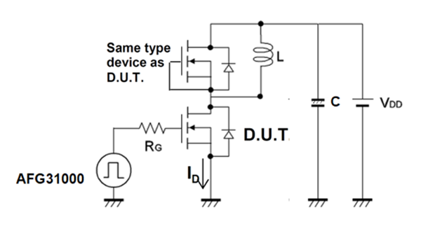
The double pulse test is performed using two components.
One is the Device Under Test (DUT) and the other is usually of the same type as the DUT.
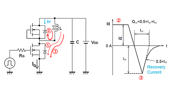
Note the inductive load on the "top" side of the circuit - the inductance is used to simulate conditions that may occur in the inverter design.
Measurement devices used include:
- power supply or SMU (Source Measure Unit),
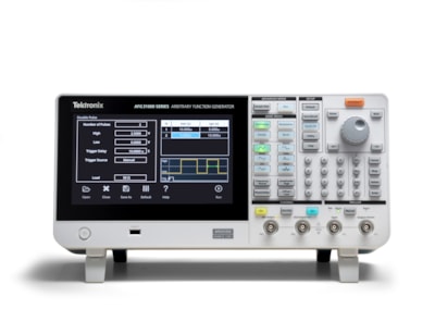
- Arbitrary Function Generator (AFG) to generate pulses that switch the MOSFET gate and initiate current conduction,
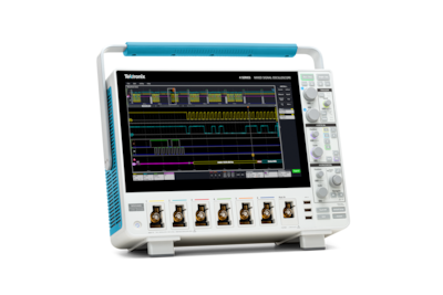
- an oscilloscope to measure the resulting waveforms.
How to generate gate control signals for the test
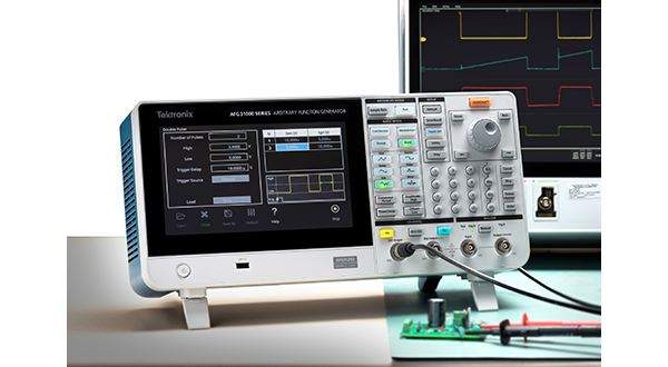
The simplest way to generate the gate control signals to perform a double pulse test is to use an arbitrary function generator (AFG). The AFG can be used to generate the gate control signal needed for the test. The Tektronix AFG31000 can be extended with a free Double Pulse Test setting that allows you to easily generate pulses of different widths.
How to measure turn-on and turn-off times and energy loss
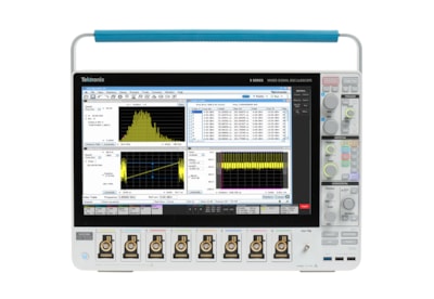
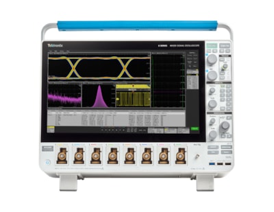
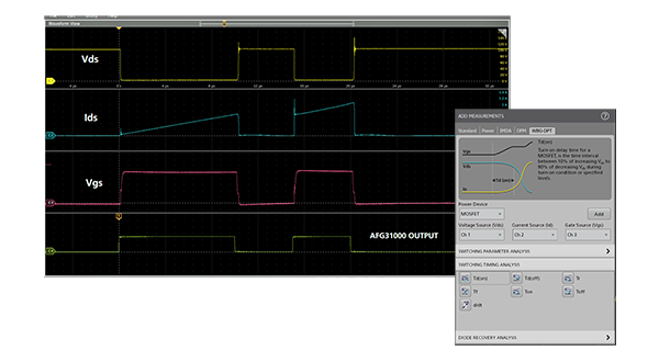
The oscilloscope is the ideal tool for capturing double pulse waveforms to determine the parameters of the on and off times of the component under test. With Tektronix 4/5/6 B Series oscilloscopes and Wide Bandgap Double Pulse Test (Opt. WBG-DPT) application software, you have all the necessary functions at your fingertips. The WBG-DPT option offers automatic measurement of switching, timing and diode back-recovery parameters according to JEDEC and IEC standards.
Reverse Recovery Measurement
The diode reverse recovery time is an indicator of the diode switching speed and therefore a factor that affects switching losses in the inverter design. Reverse current recovery occurs when the second pulse is switched. As seen in the diagram, the diode conducts current in the forward direction during phase 2.
When the lower MOSFET recloses, the diode should immediately go into blocking (reverse) mode, but for a short period of time it still conducts current in the reverse direction - this is called reverse recovery current. This current represents energy losses that directly affect the efficiency of the power converter.